What DRC errors actually mean on your first board
Clearance, annular ring, and unrouted nets, explained in plain terms, plus what each one does to a board once it reaches the fab house.
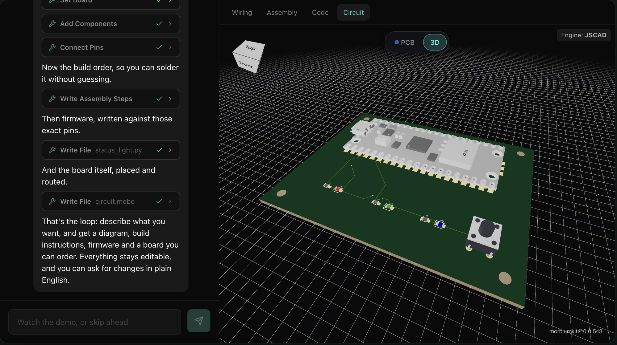
Design rule checking is the step between a board that looks finished and a board that can be made. The messages are terse, and on a first project they read like the tool is being difficult. Mostly it is telling you something a fab house would otherwise tell you three weeks later, for money.
Here are the ones you hit first.
Clearance violation
Two pieces of copper are closer together than the manufacturer can reliably separate. Etching is a chemical process with tolerances, so traces that sit too close can bridge and short.
Typical low-cost fabs want 0.15 mm or more between anything and anything. The fix is usually to move a trace, not to argue with the number.
Annular ring too small
A via or a through-hole pad has too little copper left around the drilled hole. Drills wander slightly. If the ring is thin, the drill can break out through the edge of the pad and the connection is gone.
Widen the pad, or use a smaller drill.
Unrouted net
Two pins that your schematic says are connected have no copper joining them. This is the one that quietly ruins a board: it fabricates perfectly and does nothing. Worth treating as an error rather than a warning.
Silkscreen over pad
Ink printed on a pad that should be bare metal. It does not stop the board being made, but it can interfere with solder wetting on the pad. Move the label.
Why Morbium runs these before you export
A board leaves Morbium with the checks already run, because the cost of finding a clearance problem is a few seconds during design and several weeks after fabrication. When a check fails you get the rule that was broken and the location, so the fix is a move rather than a hunt.
← All posts